

Canon is looking to produce a multi-layer image sensor with high speed, resolution and low power consumption

Typically, image sensor manufacturers have to choose between speed and resolution, while paying special attention to sensor energy consumption. According to Petapixel , Canon seems to be trying to find a way to produce a fast, high-resolution, low-power sensor.
Canon has patented a kind of sensor with a different design. According to experts, the higher the speed or resolution of the sensor, the more energy it must reach. In addition to clarity and speed, sensor energy consumption also depends on the system that the manufacturer designs for energy delivery. Canon’s patent for this type of sensor seems very ambitious.
“In recent years,” several pixels related to the imaging element have become more advanced, and as a result, the signal reading time of the pixels has become longer; “So one of the demands is to increase the reading speed of the pixel signal.”
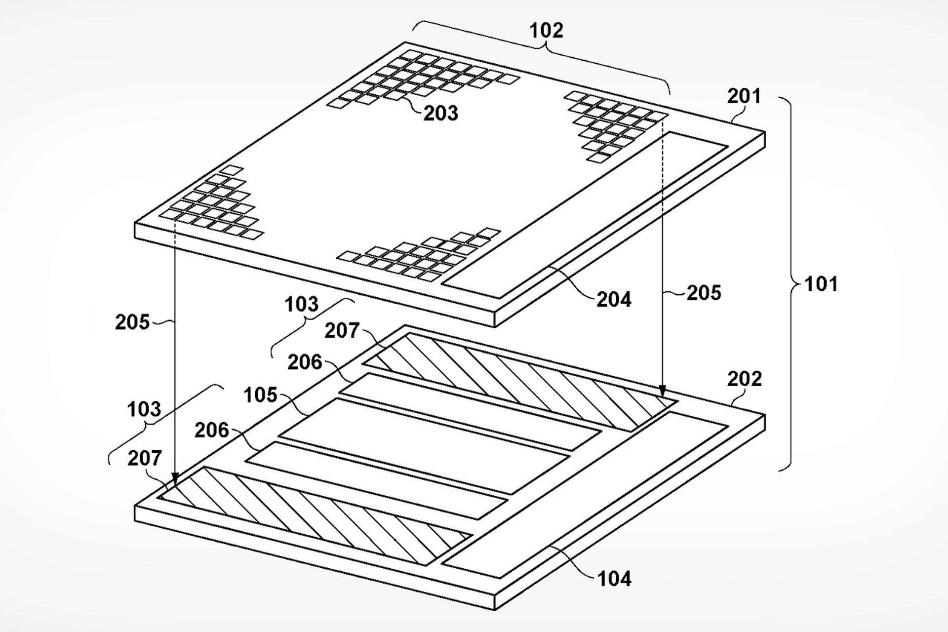
Canon’s new sensor has a multi-layer design, and items 201 and 202 form layers.
Canon says that the image sensor number 101, which belongs to the category of solid state sensors, has a multi-layered structure that includes the first bed (201) and the second bed (202). The first platform consists of a unit of pixels (102) or, in fact, an array of pixels comprising 203 units. Item 204 is actually a control unit and manages pixels.
Patents always have explanations that seem incomprehensible at first glance, and it is very difficult to extract meaningful and practical details from them. But as Canon News explains, the bottom layer of the sensor is equipped with an analog-to-digital converter (ADC) that can convert analog pixel values to digital values. This layer appears as a memory to store values and of course Black Level Correction.
Canon says the sensor shown in the patent has the ability to read the pixel signal at high speeds. This type of design increases the number of vertical output lines per pixel row, and as a result, the number of DC circuits to be connected increases and energy consumption increases.
In practice, increased energy consumption in Live View shooting greatly affects the number of shots a photographer can take. In addition, the greater the number of vertical output lines per pixel row, the higher the scale of the correction circuit; This balances the decrease in pixel signals and the excessive increase due to vertical output lines. The correction circuit is located behind the image sensor.
- Canon Patent; Handheld camera similar to DJI Osmo
- Canon Patent; Remove the camera shutter button and use the shutter touchpad
If the sensor normally can not cope with the excessive increase of vertical output lines, it is necessary to place a correction circuit on it. In the Canon system, there is also a need to add memory to store correction values. At the same time, energy consumption increases due to the speed of reading and writing memory, and it becomes more and more as time goes on.
The sensor that Canon has shown in the patent is designed with knowledge of all these problems, and one of its goals is to achieve a product that not only reads the signal of the pixels at high speed, but also reduces energy consumption.
It’s not clear that this interesting Canon idea is really practical, and there is no guarantee that it will eventually become a real sensor and be used in cameras; But thanks to the patent, we can understand what Canon’s experts are currently working on.


